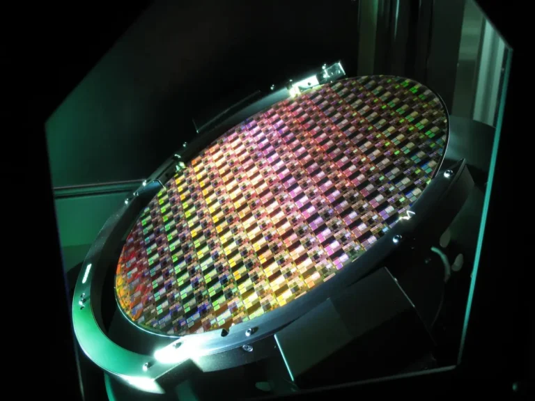
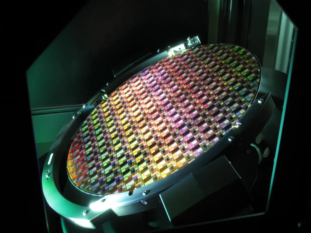
Kepler Computing, a San Jose-based semiconductor startup founded by a specialized team of physicists and computer scientists, has officially transitioned out of stealth mode after more than seven years of research and development aimed at fundamentally redesigning computer memory architecture. The company’s emergence comes at a critical juncture for the global technology industry, which is currently grappling with a severe shortage of high-performance memory chips—a bottleneck primarily driven by the exponential growth of generative artificial intelligence and high-performance computing (HPC) applications. By utilizing a proprietary new material system and an innovative 3D-stacking approach, Kepler Computing aims to increase memory density and efficiency without the traditional reliance on prohibitively expensive extreme ultraviolet lithography (EUV) equipment, potentially offering a faster and more cost-effective route to scaling the next generation of AI hardware.
The Architecture of a New Memory Standard
Since its inception in 2018, Kepler Computing has focused on solving what many industry analysts refer to as the "Memory Wall"—the growing performance gap between high-speed processors and the memory systems that supply them with data. As AI models like ChatGPT and other large language models (LLMs) grow in complexity, the demand for High-Bandwidth Memory (HBM) has surged. Traditionally, increasing the density of memory chips has required manufacturers to utilize EUV lithography, a process dominated by the Dutch firm ASML. EUV machines, which can cost upwards of $350 million each, allow for the etching of incredibly fine features on silicon, but their high cost and limited supply have become a major constraint for the industry.
Kepler’s approach bypasses this bottleneck by focusing on verticality and material science rather than just horizontal shrinking. The startup claims its "3D stacking" methodology allows it to achieve the density of 2-nanometer or 3-nanometer chips while utilizing existing semiconductor fabrication plants (fabs) that operate on more mature, less expensive nodes. This is achieved through the use of ferroelectric materials, which possess a spontaneous electric polarization that can be reversed by the application of an external electric field. By integrating these materials into a new class of memory, Kepler asserts it can read and write data at significantly lower voltages than current industry standards, reducing energy consumption and heat generation—two of the primary hurdles in modern data center design.
Strategic Funding and Government Backing
The ambitious scope of Kepler’s mission is reflected in its significant financial backing. To date, the startup has raised approximately $468 million from a diverse group of high-profile investors. The roster includes industry heavyweights such as Intel Capital, AMD Ventures, and GlobalFoundries, as well as the British investment firm Baillie Gifford. Notably, Bill Gates has also contributed through his private Gates Frontier fund, signaling the perceived importance of this technology for the future of global computing infrastructure.

In addition to private capital, Kepler has secured a pivotal commitment from the public sector. In July 2024, the United States Department of Commerce announced a letter of intent to provide Kepler with up to $245 million in federal funding. This investment, facilitated through the CHIPS and Science Act, is intended to support the development of a domestic supply chain for high-performance AI memory. The Department of Commerce highlighted Kepler’s "innovative 3D and ferroelectric technologies" as a key component in maintaining U.S. leadership in the semiconductor sector. This government support underscores the geopolitical significance of Kepler’s work, as nations race to secure the hardware necessary to power the next decade of AI innovation.
Operational Timeline and Manufacturing Partnerships
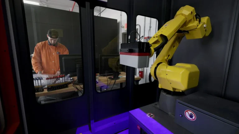
Kepler’s path to market is closely tied to its partnership with GlobalFoundries, one of the world’s largest contract chip manufacturers. GlobalFoundries has not only invested $50 million in the startup but has also provided the facilities necessary for Kepler to prove its technology at scale. For the past two years, Kepler has been operating what it calls "mini fabs" within GlobalFoundries’ facilities in Singapore and Burlington, Vermont. These specialized lines are used to produce Kepler’s memory components in conjunction with GlobalFoundries’ 28-nanometer process technology.
The company has established a clear roadmap for the coming years:
- Late 2024: Kepler plans to ship its first engineering samples of HBM chips to prospective partners and customers for evaluation.
- 2025: The company intends to ramp up production volumes at its Singapore-based facilities to meet immediate global demand.
- 2028: Kepler aims to initiate full-scale chip production within the United States, fulfilling the objectives set forth by its agreement with the Department of Commerce.
This timeline is aggressive but necessary, according to Kepler CEO and co-founder Debo Olaosebikan. He noted that while the company originally intended to focus first on Static Random Access Memory (SRAM)—the high-speed cache memory found inside CPUs and GPUs—the "explosion of demand" following the public release of ChatGPT in 2022 forced a shift in strategy. Kepler is now developing its SRAM and HBM solutions in parallel to address the immediate needs of the AI market.
Addressing the Economics of Semiconductor Fabrication
The economic argument for Kepler’s technology is as compelling as the technical one. Building a state-of-the-art semiconductor fab from the ground up currently costs between $20 billion and $40 billion and can take up to five years to become fully operational. In contrast, Kepler claims its technology can be integrated into existing fabs with a relatively modest retooling process.

According to company data, Kepler can convert a traditional fab into a "next-generation" facility in approximately eight months. This rapid turnaround time is a significant advantage in a market where demand can fluctuate wildly. By pushing existing architectures to their physical limits through material innovation rather than lithographic shrinking, Kepler offers a way for manufacturers to increase capacity without the multi-billion-dollar price tag of a new facility. Ed Kaste, Senior Vice President of GlobalFoundries’ CMOS business, emphasized that Kepler’s approach sits at the "sweet spot" of the industry’s needs, offering multigenerational scaling potential without requiring a total overhaul of existing manufacturing systems.
Technical Hurdles and Market Skepticism
Despite the promise of Kepler’s technology, the road to full-scale commercialization is fraught with challenges. One of the primary concerns for any new semiconductor material is contamination. Kepler’s composite materials include iron, a substance that is notoriously difficult to manage within a sterile fabrication environment. If iron particles were to escape into other parts of a production line, they could ruin millions of dollars’ worth of silicon wafers.
To mitigate this, Kepler and GlobalFoundries must ensure that the new materials are either processed on dedicated equipment or fully encapsulated throughout the production flow. "The art is in keeping that material really well isolated," Kaste noted, acknowledging that while the fundamental breakthroughs have been achieved, the industry still needs to see consistent results across thousands of wafers and millions of individual devices.
Furthermore, Kepler is entering a highly competitive landscape. Established giants like SK Hynix, Samsung, and Micron are already investing tens of billions of dollars to expand their own HBM production lines. While these companies are currently reliant on traditional lithography, they possess vast resources and established relationships with major customers like NVIDIA. Kepler must prove not only that its technology works but that it can be produced with the reliability and yield rates required by the world’s most demanding tech companies.
Broader Impact on the AI Ecosystem
The implications of Kepler’s success would extend far beyond the balance sheets of its investors. If Kepler can successfully deliver HBM that is as energy-efficient as SRAM, it would fundamentally change how AI models are trained and deployed. High energy consumption is currently one of the greatest costs associated with AI data centers, leading to massive electricity demands and environmental concerns. A significant reduction in the voltage required for memory operations would allow for more powerful AI models to run on existing power grids.

Moreover, by reducing the reliance on EUV lithography, Kepler could help democratize the production of high-end semiconductors. If cutting-edge density can be achieved on 28-nanometer or 14-nanometer equipment, it could lower the barrier to entry for other specialized chip designers and reduce the global dependency on a single equipment supplier.
Conclusion: A Pivot Point for the Industry
As Kepler Computing moves toward its 2025 production goals, the semiconductor industry will be watching closely. The startup’s ability to "solve the physics problem" of memory scaling through material science represents a bold departure from the industry’s decades-long adherence to Moore’s Law via lithographic shrinking.
With nearly half a billion dollars in funding and the backing of the U.S. government, Kepler has the resources to attempt a disruption of the memory market. However, in the semiconductor world, innovation is only half the battle; the true test lies in the ability to scale. As Austin Lyons, a chip analyst for Creative Strategies, observed, the ultimate question is whether Kepler’s innovation can be used at a scale that makes it worth the cost of the transition. If Kepler can bridge that gap, it may well provide the foundation for the next era of accelerated computing.
About the Author