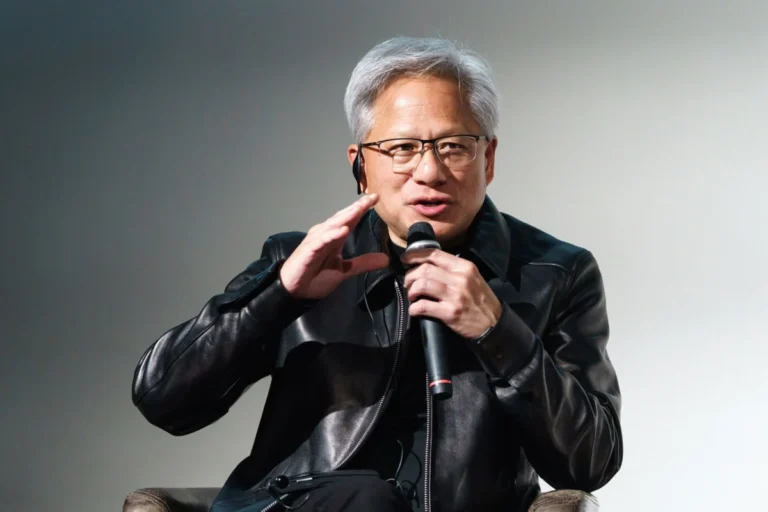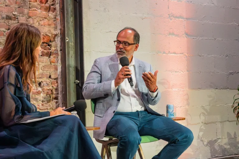

Following his high-profile departure as the Chief Executive Officer of Intel Corporation in late 2024, Pat Gelsinger has embarked on a strategic pivot into the world of venture capital, seeking to address the fundamental physical limitations currently facing the semiconductor industry. Gelsinger, a veteran of the silicon industry who spent decades at Intel and served as the CEO of VMware, has officially joined Playground Global as a general partner. This move marks a significant transition for one of the most recognizable figures in technology, moving from the helm of a Fortune 500 manufacturing giant to the agile, high-risk environment of deep tech investment.
Gelsinger’s transition was characterized by a deliberate and exhaustive "100 meetings in 100 days" strategy. This period of reflection and consultation was designed to distill a lifetime of engineering and executive experience into a focused mission for the final act of his career. By March 2025, Gelsinger concluded that his future lay not in the administrative rigors of public company management or the high-stakes world of private equity, but in the foundational science of "deep tech"—specifically, the hardware and physics required to sustain the progress of modern computing.
The Strategic Shift from Public Executive to Venture Partner
The decision to join Playground Global, a firm known for its focus on complex engineering and scientific breakthroughs, was driven by Gelsinger’s desire to escape the quarterly pressures of Wall Street. During his tenure at Intel, Gelsinger was tasked with a massive turnaround effort, attempting to regain the company’s manufacturing lead while navigating the geopolitical complexities of the global chip shortage. In his new role, he has indicated a preference for the "cool tech" over the "big checks" associated with private equity firms.
Gelsinger’s arrival at Playground Global coincides with a broader shift in the venture capital landscape. As artificial intelligence continues to disrupt the traditional software-as-a-service (SaaS) model, investors are increasingly looking toward the physical layer of the technology stack. The hardware required to train and run massive large language models (LLMs) has become the new bottleneck of innovation, creating a fertile ground for startups specializing in semiconductors, photonics, and advanced materials. Gelsinger’s thesis is that while many firms are now chasing deep tech, few possess the institutional memory and technical depth required to distinguish between genuine scientific breakthroughs and overly ambitious laboratory experiments.
A Chronology of Transition: From Intel to Playground Global
The timeline of Gelsinger’s transition reflects a rapid but calculated move from corporate leadership to investment strategy:
- Late 2024: Pat Gelsinger departs Intel Corporation after a tenure focused on the "IDM 2.0" strategy, which aimed to open Intel’s factories to outside customers.
- Late 2024 – Early 2025: Gelsinger conducts a "100 meetings in 100 days" tour, consulting with leaders in academia, government, and the private sector to determine his next move.
- March 2025: Gelsinger officially joins Playground Global as a General Partner. He also accepts a board seat at xLight, a portfolio company specializing in advanced lithography.
- June 2025: The United States Department of Commerce, through the National Institute of Standards and Technology (NIST), announces a finalized CHIPS Act incentive package for xLight, signaling federal support for the technologies Gelsinger is championing.
- July 2025: Gelsinger appears at the RAISE Summit in Paris, outlining his vision for the future of the semiconductor industry and the necessity of "reawakening" Moore’s Law.
The Quest to Reanimate Moore’s Law
At the heart of Gelsinger’s new mission is the survival of Moore’s Law. Proposed by Intel co-founder Gordon Moore in 1965, the law posits that the number of transistors on a microchip doubles approximately every two years, leading to exponential increases in processing power and decreases in cost. For decades, this principle served as the heartbeat of the global economy. However, as transistor features approach the size of individual atoms, the semiconductor industry has encountered a "physics wall."
Shrinking transistors further using traditional methods has become prohibitively expensive and technically daunting. The industry currently relies heavily on Extreme Ultraviolet (EUV) lithography, a technology dominated by the Dutch firm ASML. ASML’s machines, which use 13.5-nanometer wavelength light to etch patterns onto silicon, are among the most complex instruments ever built, costing upwards of $350 million each.
Gelsinger believes that the next leap in performance will not come from incremental improvements to existing platforms but from radical advances in lithography. This is where his involvement with xLight becomes critical. By focusing on novel light sources and etching techniques, Gelsinger and the team at Playground Global aim to provide the tools necessary to pack even more features onto silicon wafers, effectively extending the lifespan of Moore’s Law into the next decade.
Supporting Data: The Trillion-Dollar Semiconductor Market
The economic stakes of Gelsinger’s venture are immense. Data from industry analysts and the Semiconductor Industry Association (SIA) suggest a massive acceleration in market growth:
- Market Valuation: In early 2024, the global semiconductor market was projected to reach $1 trillion in annual revenue by 2030. However, the explosive demand for AI accelerators, such as those produced by Nvidia and AMD, has pulled that timeline forward significantly.
- Accelerated Growth: Revised estimates now suggest the industry could hit the $1 trillion mark as early as 2026 or 2027. Gelsinger noted that the sheer scale of the market means that even startups capturing a small percentage of the total addressable market (TAM) can achieve extraordinary returns for investors.
- The AI Multiplier: AI workloads require specialized silicon that prioritizes high-bandwidth memory and massive parallel processing. This has created a "Cambrian explosion" of new chip architectures, many of which are being funded by venture firms like Playground Global.
- Capital Intensity: The cost of developing a leading-edge 2-nanometer chip design is estimated to exceed $500 million, while a new "mega-fab" (semiconductor fabrication plant) can cost $20 billion. This capital intensity underscores the need for strategic investment from both the private sector and government entities.
Government Intervention and the CHIPS Act
Gelsinger’s move into deep tech is also deeply intertwined with national security and industrial policy. The US government’s stance on semiconductors has shifted from a hands-off approach to one of active intervention via the CHIPS and Science Act. The investment in xLight, a company Gelsinger now helps oversee, is a direct result of this policy.
The Department of Commerce’s decision to finalize incentives for xLight highlights a strategic interest in securing the domestic supply chain for lithography. Currently, the reliance on a single foreign supplier (ASML) for EUV technology represents a significant single point of failure for the US tech ecosystem. By fostering domestic startups that can innovate in the lithography space, the US aims to build a more resilient and competitive semiconductor industry.
Gelsinger’s background as a CEO who frequently lobbied for the CHIPS Act makes him a unique bridge between the startup world and Washington D.C. His ability to navigate the "Triple Helix" of innovation—industry, government, and academia—is viewed as a major asset for Playground Global.
Broader Impact and Industry Implications
The implications of Gelsinger’s new career path extend beyond his personal portfolio. His move signals a maturation of the venture capital industry, where technical expertise is becoming as valuable as financial acumen.
For the broader technology sector, Gelsinger’s focus on lithography suggests that the "software-defined world" is once again becoming a "hardware-constrained world." As AI models grow in complexity, the efficiency of the underlying silicon becomes the primary differentiator for performance. If Gelsinger’s bets on xLight and other deep tech firms pay off, it could lead to a new era of decentralized semiconductor innovation, breaking the near-monopolies currently held by a few global giants.
Furthermore, Gelsinger’s departure from the public market highlights a growing trend of top-tier executive talent seeking "impact" over "administration." By choosing to work with founders at the "edge of science," Gelsinger is positioning himself at the center of the next industrial revolution. His belief that "God said, ‘Let there be light’" reflects his spiritual and professional conviction that photonics and lithography are the keys to unlocking the next stage of human progress.
In the coming years, the success of Gelsinger’s tenure at Playground Global will be measured not just by financial returns, but by whether the startups he mentors can successfully navigate the "valley of death" that claims so many hardware companies. If they succeed, they will not only validate Gelsinger’s deductive career process but also ensure that the foundational law of the digital age—Moore’s Law—remains a reality for the foreseeable future.
About the Author